Filter circuits
From the
previous discussions, it was found that the output of rectifier is pulsating D.C.
i.e. it contains A.C. and D.C. of components. The A.C. component is undesirable
and must be kept away from the load. The filter circuit is used to remove the
a.c. component and to allow only the D.C. component to reach the load. Obviously,
a filter circuit should be installed between the rectifier and the load.
Types of
filter circuits
1.
Capacitor filter
The below fig
shows a capacitor filter. It consists of a capacitor placed across the
rectifier output in parallel with load. The pulsating direct voltage of the
rectifier is applied across the capacitor. As the rectifier voltage increases
to Vm it charges the capacitor and supplies current to the load. During this period
(first quarter cycle) of voltage the diode is forward biased.

(a) Half wave Rectifier with Capacitor Filter

(b) Capacitor filter with centre tapped full wave rectifier
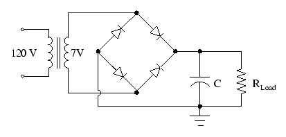
(c) Capacitor filter with bridge full wave rectifier

(d) Half wave and full wave rectifier
As the input
voltage reaches its peak value, the diode stops conducting because now the
diode is at effective zero bias condition because of applied voltage of +Vm at
anode and voltage across charge capacitor +Vm at cathode. So the diode now acts
also as the open switch. Since the source voltage slightly less than Vm, the
diode goes in to reverse bias. Hence the output stays at the voltage across
capacitor. With the diode now open, the capacitor discharges through the load resistance.
The discharging time constant (RLC) is much greater than the period
of the input signal. So the capacitor will lose only a small part of its charge
during the off time of the diode.
When the source
voltage again reaches its peak, the diode conducts briefly and recharges the
capacitor to the peak value and the process is repeated continuously. Thus we
get load voltage which is very nearer to a perfect D.C.
The capacitor
filter circuit is extremely popular because of its low cost, small size, little
weight and good characteristics. For small load currents, this type of filter
is preferred.
Choke input
filter or LC filter
The choke
input filter consists of an inductor and a capacitor as shown in below fig.
here the output from the rectifier is directly fed to the inductor which is
connected in series with the rectifier. The choke allows the D.C. component of
rectifier output passes easily through the inductor. Since the capacitor works
as an open circuit for D.C., all D.C components of rectifier output will
present at the output across the load resistor. Since the D.C. resistance of
the inductor is very small, a negligible drop occurs at this inductor. So we
can say that all the D.C. output of rectifier appears as the output.

(a) Choke Input Filter

(b) Output Waveform of Choke Input Filter
Form the A.C
point of view it can be understood that the reactances of inductor and
capacitor are low and high respectively for the fundamental frequency of the
A.C component of 100 HZ for
full-wave rectifier. So the A.C current has the difficulty in passing through
the inductor. Even though some A.C current passes through the inductor, it will
pass through the capacitor.
In this way,
the filter circuit has filtered out the A.C component from the rectifier
output, allowing D.C component to reach the load.
CLC filter or
pie filter
The filter
consists of a filter capacitor connected across the rectifier output, a choke L
in series and another filter capacitor connected across the load. Only one
filter section is shown in below fig but several identical sections are often
used to improve the smoothening action. The pulsating output from the rectifier
is applied across the input terminal of the filter.

(a) CLC Filter

(b) Output Waveform Of CLC Filter
(a)
The filter capacitor offers low
reactance to A.C component of rectifier output while it offers infinite
reactance to the D.C component. Therefore, capacitor passes appreciable amount
of A.C component while the D.C component continues its journey to the choke.
(b)
The choke offers high reactance to
the A.C component but it offers almost zero reactance to the D.C component. Therefore,
it allows the D.C component to flow through it, while the unbypassed A.C
component is blocked.
(c)
The filter capacitor by passes the
A.C component which the choke has failed to block. Therefore, only D.C
component appears across the load that is what we desire.
No comments:
Post a Comment